I designed a PCB by talking to an agent

I have never designed a PCB before.
There is now a 70 × 90 mm two-layer board sitting in my pcb/ folder with clean Gerbers, an Excellon drill file, a pick-and-place CSV and a bill of materials, ready to zip and send to JLCPCB. DRC passes at zero errors.
I did not learn KiCad to do it. I described what I wanted, and an agent drove KiCad through an MCP server.
That sentence is either exciting or annoying depending on your priors, so let me be specific about what actually happened — including the parts where it was wrong.
What the board is
The Buddy project lived on a breadboard for months. Breadboards are wonderful until they are not: a jumper works its way loose, you lose an evening to a fault that is not in your code, and the SPI clock has to stay at half speed because the wiring cannot take more.
So the board is a carrier, not a soldered assembly. Every module — the DevKit, the display, the microphone, the amplifier, the gyro — drops into a female 2.54 mm header socket. Nothing gets soldered to the modules. If a part dies or I want to swap the display, I pull it out.
The design constraint that mattered was: the same parts I prototyped with must drop straight in. No new BOM, no surface-mount, no reflow.
How it went
The loop was conversational. I described the physical layout I wanted — USB pointing down, display on the front face so it looks out through the chassis aperture, everything else on the back, mounting holes at the corners — and the agent placed footprints, assigned nets from the existing circuit diagram, poured ground on both layers, and ran Freerouting over the signals.
Then DRC. Then fix. Then DRC again.
The thing that made this work is that PCB design has a machine-checkable definition of wrong. Design rule checking is a real oracle: clearance violations, unconnected nets, courtyard overlaps. The agent could propose something, get told precisely how it was broken, and iterate — which is exactly the loop where these tools are strongest and exactly the loop that most software tasks lack.
Final state: 0 DRC errors, 8 warnings, all of them cosmetic and all on the mounting holes.
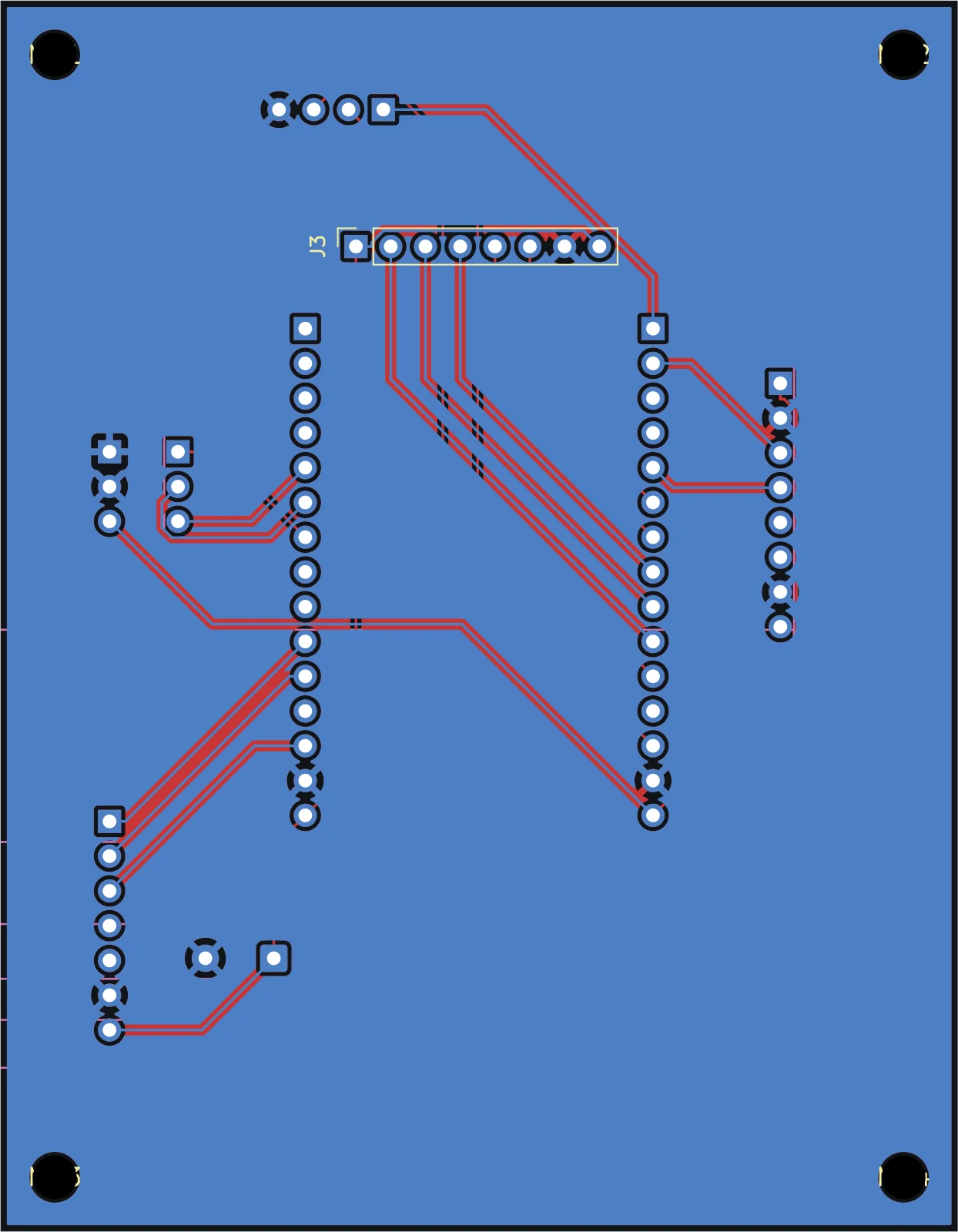
The four things it got wrong
This is the useful part, and it is why I would not tell you to send a board to fab because a model said it was fine.
1. The DevKit row spacing is an assumption. The two 15-pin socket rows sit exactly 25.4 mm apart. That is the common spacing — but the DOIT DevKit V1 ships in a couple of different widths, and nothing in the pipeline measured my actual board. If mine is not 25.4 mm, the sockets do not line up and the board is scrap.
2. Every module pin order is an assumption. The socket-to-module pin mapping follows the layouts you usually find on the blue ST7735, the purple INMP441, the GY-521 and the MAX98357A. “Usually” is carrying a lot of weight there. These modules get cloned by a dozen manufacturers and the silkscreen is the only ground truth. (Because they are sockets, a mismatch is survivable with short jumpers — which is an argument for sockets, not for trusting the mapping.)
3. The antenna keep-out was not cut. The ESP32’s PCB antenna wants no copper underneath it. The automatic ground pour filled that area anyway, because pouring ground everywhere is the correct default and knowing that this specific rectangle is an exception requires knowing what an antenna is. The DevKit sits about 10 mm up on its sockets so the practical impact is reduced, but it is a real defect and it is mine to fix.
4. Power traces are 0.2 mm. That is the autorouter’s default and it is fine for a USB-powered board with a bulk capacitor and two ground planes. It is also not a decision anybody made. The 5 V feed to the amplifier deserves to be wider, and nothing in the process was going to volunteer that.
What I actually think about this
Three of those four failures have the same shape. The agent was excellent at the rules it could check and blind to the physical world it could not.
DRC catches clearance and connectivity. It does not know how wide the board in your drawer is, what the silkscreen on your particular microphone breakout says, or that a rectangle of copper under one specific corner will quietly cost you WiFi range. Every one of those needs someone to look at a physical object.
So the honest description is not “an agent designed my PCB.” It is: an agent did about a day of tedious, error-prone footprint placement and net assignment in twenty minutes, got it structurally right, and left me with a short list of physical-world checks that I am well able to do with a ruler.
That is a very good trade. It is not the same as the tool being an engineer.
For what it is worth, this is the same conclusion I keep reaching everywhere else: these things are transformative exactly where there is a fast, honest feedback signal — a compiler, a test suite, a DRC report — and they are confidently wrong the moment the feedback loop opens up and the ground truth is a physical object in a drawer.
Before it goes to fab
The four items above, in order, with a ruler and my actual modules on the desk. Then widen the power nets, cut the antenna keep-out, re-pour, re-run DRC.
Then I will find out whether any of this survives contact with a soldering iron. I will write that one too, especially if it goes badly.
The KiCad project, Gerbers and full pin map are in esp32-buddy under pcb/. Built with KiCad 10 driven through the KiCad MCP server, signals autorouted with Freerouting.